Oplexa Edge 1
A purpose-built transformer inference processor - a custom instruction set, an on-chip dataflow engine, and a compiler that maps model layers directly to silicon, instead of routing them through a general-purpose GPU pipeline they were never designed for.

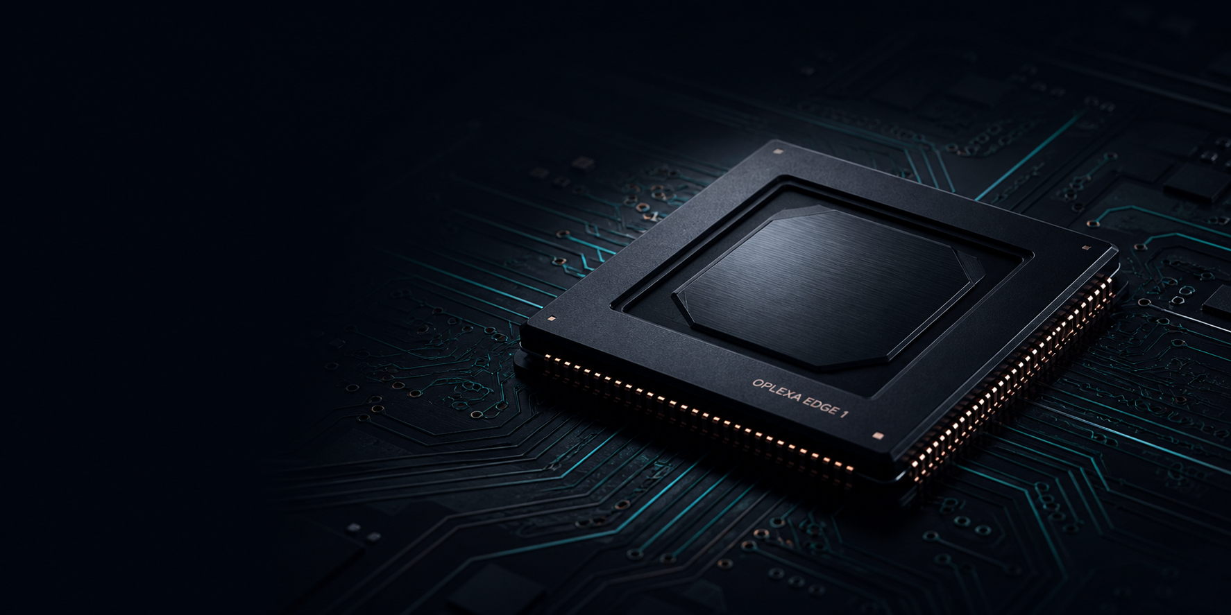
Rather than adapting a legacy GPU or NPU vector pipeline, Oplexa Edge 1 uses a tailored execution pipeline built explicitly for attention mechanics, KV-cache reuse, token generation, and low-bit quantization - running on an instruction set Oplexa designed and owns, with a compiler and software stack built to be compatible with the model formats and tooling teams already use, so adopting Edge 1 doesn't mean rebuilding a software stack from scratch.
Custom Transformer ISA
An instruction set designed around attention and token generation, not general-purpose matrix math - eliminating the compute overhead a GPU carries for workloads it isn't running.
On-Chip Dataflow Engine
Minimizes off-chip DRAM access to hit ultra-low power envelopes without sacrificing throughput on the operations that matter for inference.
Hardware-Software Co-Design
A direct compilation toolchain mapping model layers straight to execution units, part of a software ecosystem designed to interoperate with existing ML frameworks rather than requiring a full replacement.
Static Scheduled Execution
A deterministic execution flow that removes microarchitectural jitter, enabling predictable, microsecond-scale response times - the property real-time and safety-relevant deployments actually require.
The core of Oplexa Edge 1 is a grid of processing elements, currently being proven out at 8x8 scale in a cycle-approximate simulator. Each cell executes a fixed, compile-time-scheduled slice of the transformer's matrix operations - no runtime dispatch, no dynamic scheduler deciding what runs next.
| Parameter | Datacenter GPU | Edge CPU | Edge NPU | Oplexa Edge 1 |
|---|---|---|---|---|
| Primary Workload | Training / large-batch cloud inference | General compute | Vision / hybrid CNN | Transformer-native pure inference |
| Power Budget | 70W-700W+ | 15W-125W | 2.5W-15W | 5W-25W |
| Latency Profile | Batch-optimized, high jitter | High latency | Low latency (light workloads) | Deterministic, microsecond response |
| Deployment Footprint | High CapEx, continuous cloud bandwidth | High cost per token | Low-to-moderate modular cost | Ultra-low CapEx, air-gapped |
Autonomous Robotics & Drones
Ultra-low-latency path planning and real-time vision-language reasoning without a cloud round trip.
Defense & Smart Infrastructure
Air-gapped token processing for programs that require export-control-clean silicon and no continuous cloud connectivity.
Industrial Automation
High-FPS deterministic quality inspection and predictive maintenance on the factory floor.
Telecom
Inference at the network edge within power budgets a base station can actually support.
Private Healthcare Systems
On-device medical signal analysis that keeps regulated data on-premise.
Sovereign AI Programs
Inference infrastructure that doesn't route through a foreign hyperscaler's cloud.
Where Oplexa Edge 1 is today
Edge 1 is currently being developed through a staged validation plan: a cycle-approximate 8x8 processing-element grid simulator, followed by FPGA validation, and then an ASIC program. Architecture decisions are made early in software, where they can be measured and changed before hardware commitments become expensive.
Specifics on model support, quantization, and measured performance are shared with design partners as validation progresses.